Mayumiotero – Metasurface Optics could reshape how engineers design cameras for smartphones, wearables, medical devices, and other compact systems. For decades, cameras have relied on curved glass or plastic lenses to focus incoming light. Those lenses work extremely well. However, they also occupy physical space, especially when several optical elements must work together. Metasurfaces offer a different approach. Instead of depending only on curved components, they use carefully engineered structures that interact with light at a very small scale. As a result, researchers can explore optical components that are remarkably thin. This idea matters because modern devices continue to shrink while their cameras become more capable. Smartphone camera bumps show how difficult that balance can be. Therefore, thinner optical components could give designers more freedom. Metasurfaces are not ready to replace every traditional lens, but their progress points toward a fascinating new chapter in camera engineering.
Read Also: Alibaba’s Qwen Surges Past Meta and Google as Chinese AI Gains Global Momentum
How Tiny Nanostructures Can Manipulate Incoming Light
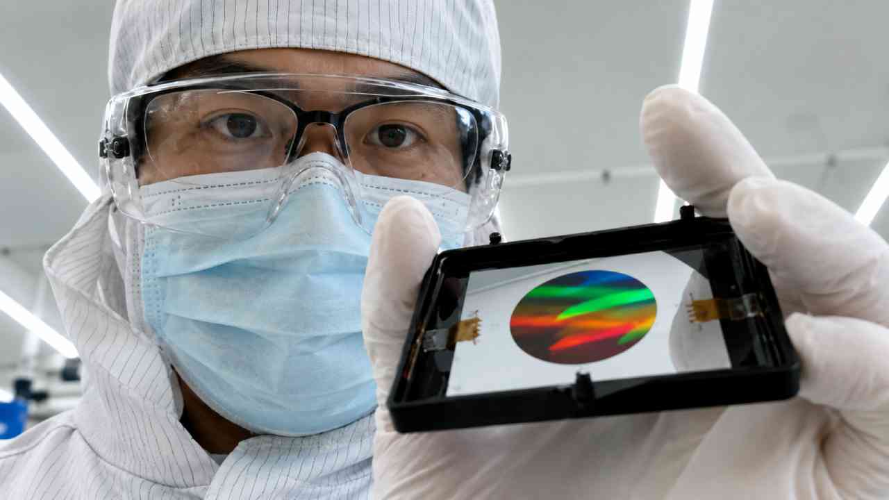
A metasurface may look flat to the human eye, yet its surface contains carefully arranged microscopic or nanoscale structures. These structures can alter properties of incoming light, including its phase and polarization. By controlling those interactions across a surface, engineers can guide light toward a desired focus. A metasurface designed for focusing is commonly associated with the concept of a metalens. In contrast, a conventional lens relies heavily on its curved shape and refractive material. This distinction makes metalenses particularly interesting for compact devices. Moreover, engineers can change the geometry and arrangement of individual structures to achieve different optical effects. The underlying physics is complex, but the basic concept is surprisingly intuitive. Rather than forcing light through several bulky curved elements, designers attempt to control it through an engineered surface. Consequently, optical design begins to resemble nanoscale engineering as much as traditional lens making.
Why Conventional Camera Lenses Still Need So Much Space
Modern camera modules are more complicated than they appear from the outside. A smartphone camera can contain several optical elements positioned between the outside world and the image sensor. Each component helps focus light or reduce unwanted optical effects. Meanwhile, manufacturers also need room for autofocus systems, stabilization hardware, filters, and the sensor itself. This explains why reducing phone thickness does not automatically produce a thinner camera module. In fact, improving image quality can create the opposite problem. Larger sensors and sophisticated lenses often require additional physical depth. Computational photography can correct many imperfections after an image reaches the sensor. Nevertheless, software cannot eliminate every optical requirement. Metasurface Optics becomes interesting in this context because it could potentially simplify certain optical functions. Instead of asking how much smaller another curved lens can become, researchers can ask whether a flat engineered surface could perform part of the same job.
Metalenses Are More Than Simply Flat Pieces of Glass
The term “flat lens” can make metalens technology sound deceptively simple. In reality, its surface geometry may contain an extraordinary level of microscopic detail. Individual structures interact with light differently depending on their size, shape, orientation, and material. Together, those interactions produce a designed optical response. Therefore, the intelligence of the component lies largely in its pattern rather than a visibly curved profile. This approach creates opportunities beyond basic focusing. Researchers are studying metasurfaces for polarization control, beam shaping, sensing, holography, spectroscopy, and other optical functions. That versatility could eventually allow engineers to combine capabilities that previously required separate components. However, laboratory demonstrations should not be confused with finished consumer products. A camera must operate reliably under many lighting conditions and across a broad range of visible wavelengths. Even so, metalenses demonstrate that an optical component does not necessarily need the familiar shape people have associated with lenses for centuries.
Smartphone Cameras Could Be an Important Test for the Technology
Smartphones represent an obvious opportunity because every millimeter of internal space matters. Manufacturers must fit batteries, processors, antennas, cooling systems, speakers, sensors, and cameras inside increasingly sophisticated devices. At the same time, consumers expect better zoom, low-light photography, portraits, and video. Consequently, camera hardware competes for valuable space. Metasurface Optics could eventually help designers reduce the size of selected optical components or introduce new sensing functions in compact packages. Yet it would be unrealistic to assume that camera bumps will suddenly disappear because of one technological breakthrough. Camera thickness depends on sensor dimensions, focal length, stabilization, aperture design, and many other factors. Therefore, early metasurface applications may complement conventional optics instead of replacing them completely. A hybrid system could be more practical. Traditional lenses could handle tasks they already perform efficiently, while metasurfaces manage specialized functions where thinness and optical control provide a meaningful advantage.
AR Glasses May Benefit Even More Than Smartphones
While smartphones provide an exciting use case, augmented reality could become an equally important field for metasurface development. AR glasses face a severe engineering challenge: users want them to look and feel like ordinary eyewear. Heavy optical assemblies work against that goal. Therefore, every reduction in component size and weight matters. Metasurfaces may help engineers manipulate light inside more compact optical architectures. They could also support sensing, beam control, or display-related functions depending on the design. In addition, wearable devices must balance image quality with comfort, battery life, heat, and appearance. This creates strong demand for optical technologies that achieve more within less space. Still, metasurfaces alone cannot solve every AR problem. Displays, eye tracking, processors, batteries, and software remain equally important. Nevertheless, the technology fits naturally into the broader effort to miniaturize wearable computing. If future AR glasses become significantly lighter, advanced flat optics may play an important role behind that transformation.
Medical Imaging and Sensors Could Offer Practical Opportunities
Consumer cameras receive plenty of attention, but specialized imaging may provide some of the most valuable applications. Medical devices, scientific instruments, robots, and industrial sensors often benefit from smaller optical systems. For example, compact imaging hardware can make portable diagnostic equipment easier to design. Likewise, robots may require several cameras and sensors without adding unnecessary weight. Metasurface Optics could contribute to these systems by enabling specialized control of light in a small footprint. Furthermore, some applications do not require the same broad photographic performance expected from a flagship smartphone camera. That distinction matters because a metasurface optimized for a specific wavelength or sensing task may be easier to implement than a universal consumer lens. Consequently, specialized markets could become important stepping stones for the technology. In my view, this is one of the more realistic paths forward. Revolutionary optical technologies often become useful first where their unique strengths solve a clearly defined engineering problem.
Color Remains One of the Hard Problems Engineers Must Solve
Creating a tiny optical component is impressive, but producing excellent full-color images introduces another level of difficulty. Different colors correspond to different wavelengths of light. Therefore, an optical design must manage those wavelengths carefully if it wants red, green, and blue details to reach the correct focus. Traditional optical systems also face chromatic aberration, but engineers have spent generations developing methods to control it. Metasurface researchers must achieve similar performance while preserving the advantages of thin structures. In addition, practical cameras need high light efficiency, useful apertures, broad fields of view, accurate manufacturing, and consistent performance. These requirements become especially demanding in mass-market devices. A technology that works under controlled laboratory conditions may behave differently when millions of units must be manufactured at acceptable cost. For that reason, progress should be judged by overall system performance rather than thickness alone. Thin optics become truly valuable only when they deliver dependable images.
Read Also: Neo-Memphis Design: A Playful Revival of Bold Geometry and Modern Creativity
Manufacturing Will Decide How Quickly Metasurfaces Reach Consumers
An advanced optical design has limited commercial value if manufacturers cannot produce it efficiently and consistently. Metasurfaces require extremely precise patterns, which makes fabrication a crucial part of their future. Fortunately, many of the techniques involved share concepts with semiconductor manufacturing and nanofabrication. That connection creates interesting possibilities for scaling production. However, large-volume consumer electronics demand exceptional yields and tight cost controls. A component may need to be produced millions of times while maintaining nearly identical optical characteristics. Moreover, manufacturers must integrate it with sensors, packaging, electronics, and existing camera systems. Therefore, commercialization involves far more than demonstrating an impressive metalens in a research environment. Progress in fabrication could be just as important as progress in optical design. If manufacturing becomes scalable, metasurface components may move from specialized systems into everyday products. Until then, conventional lenses retain enormous advantages because their production methods are mature, reliable, and highly optimized.
AI and Computational Imaging Could Strengthen Flat Optics
The future camera may not depend on optics alone. Instead, hardware and software are increasingly being designed as a single imaging system. Modern smartphones already use computational photography to combine exposures, reduce noise, improve dynamic range, and reconstruct detail. Metasurface Optics could fit naturally into this trend. For example, engineers might design a compact optical component with known characteristics and then use computational processing to compensate for specific limitations. Machine learning could further improve reconstruction when enough information reaches the sensor. This approach changes the engineering question. A physical lens may no longer need to create a perfect final image by itself. Rather, optics could capture useful information while software transforms that information into the desired result. However, algorithms cannot recover information that was never captured. Good optical efficiency and reliable sensor data remain essential. Therefore, the strongest future systems may combine advanced metasurfaces, high-quality sensors, and intelligent image processing instead of treating them as competing technologies.
Future Cameras May Look Very Different From Today’s Designs
The most exciting aspect of Metasurface Optics is not simply the possibility of making an existing lens thinner. Instead, it encourages engineers to reconsider how an entire imaging system should be built. Cameras have evolved from mechanical instruments into combinations of optics, semiconductor sensors, processors, and sophisticated software. Metasurfaces could add another layer to that evolution by bringing nanoscale engineering directly into optical design. In the near term, hybrid solutions appear more realistic than the complete disappearance of conventional lenses. Over time, however, improvements in materials, fabrication, computational imaging, and optical efficiency could expand what flat optics can accomplish. That could influence smartphones, AR glasses, medical equipment, robotics, automotive sensing, and scientific instruments. The familiar stack of curved lenses is unlikely to vanish overnight. Yet the direction is clear: future cameras may increasingly control light through engineered surfaces that are thinner, more specialized, and deeply integrated with computation.